Eclipse: Tapeout and Testing
Eclipse is an ASIC taped out in TSMC65nm technology that integrates features such as Stochastic Rounding(SR) extension, an X-interface, and a T-head DIV/SQRT unit. This project contains system integration, a complete ASIC backend process, and ASIC testing after the chip returns.
In Short
ASIC Eclipse is a chip designed to test new units including Stochastic Rounding(SR) unit, X-interface, and T-head DIV/SQRT unit.
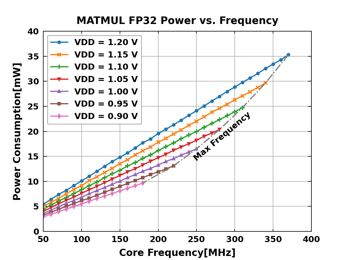
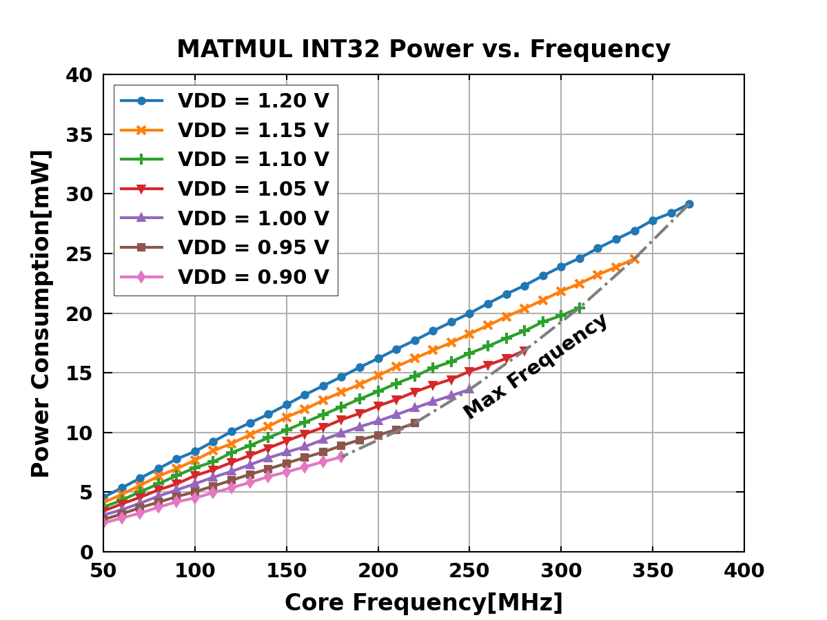
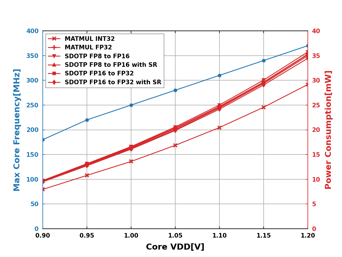
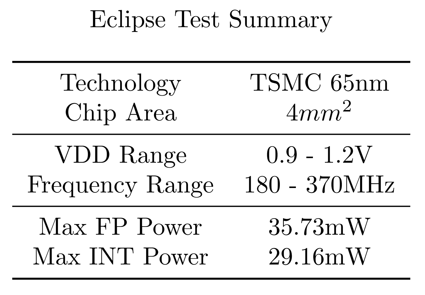
It is taped out in TSMC 65nm technology and works at 370 MHz@1.2V and room temperature on the tester. A summary of the testing is shown in the figure below. This project was carried out at IIS, ETH.
Eclipse: Architecture
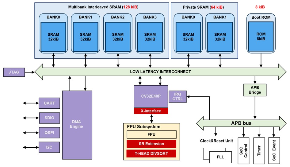
Eclipse uses the PULPissimo microcontroller architecture with an in-order RISCV core, CV32E40P, and 192 kiB on-chip SRAM. The whole SoC is in 1 power domain, and there are 2 clock domains: SoC and Peripherals. We provide a JTAG interface for testing. It is used to halt the core, load the program, configure FLL, resume the core, and check the return value after the program execution.
Eclipse: VLSI Backend
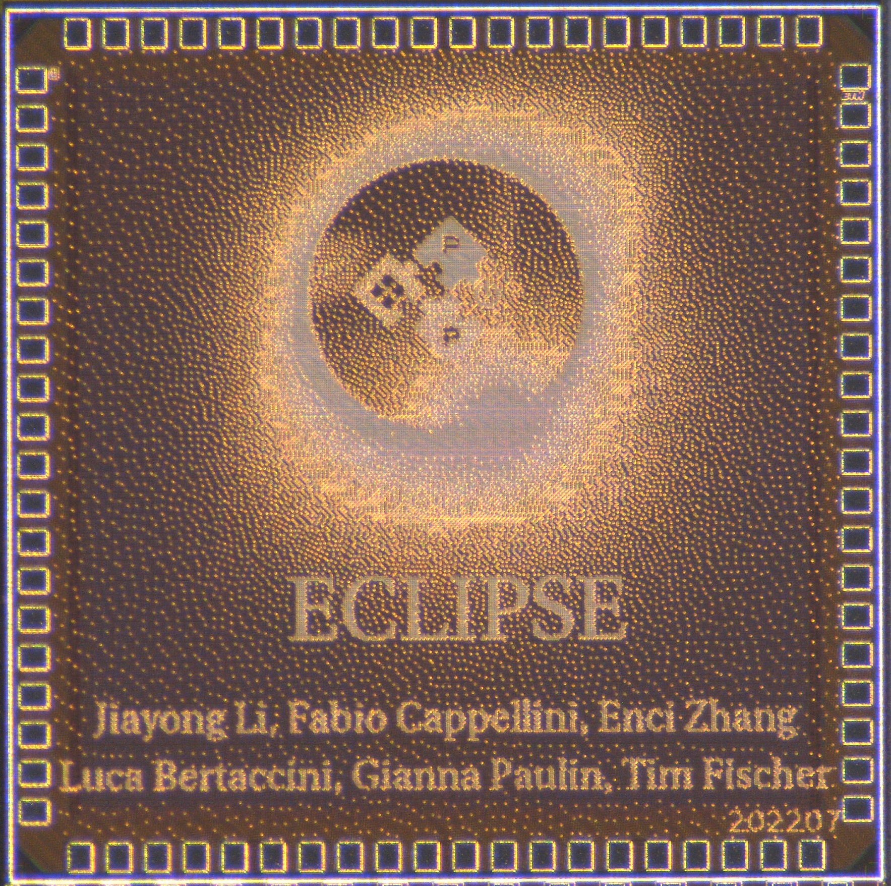
Eclipse is taped out in TSMC 65nm technology with a 2mm x 2mm die size and uses QFN56 packaging. The flowing figures shows the layout and a photo of the real silicon.

Eclipse: Testing
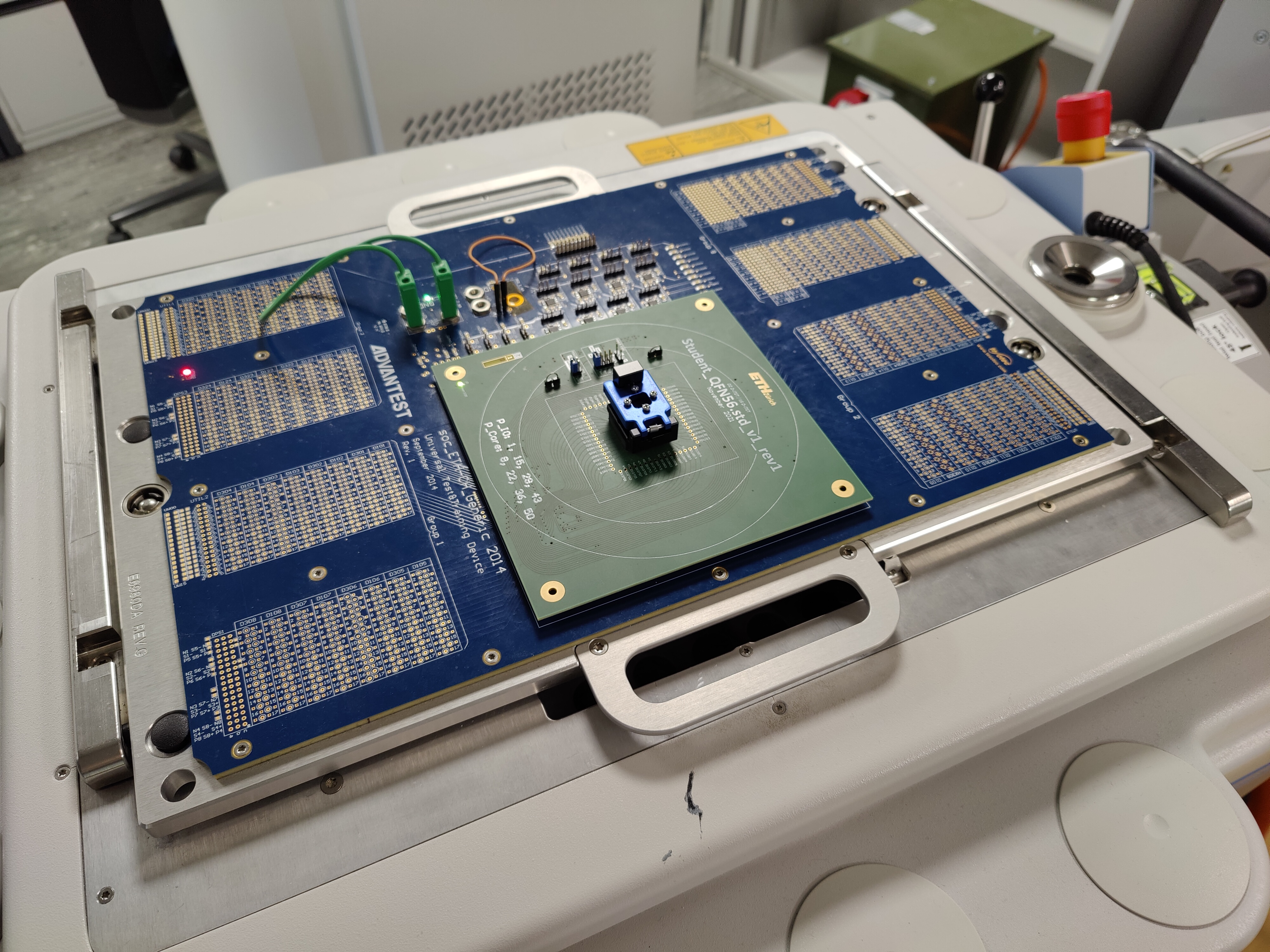
After the chip returns, it is tested on the tester for function, speed, and power.
